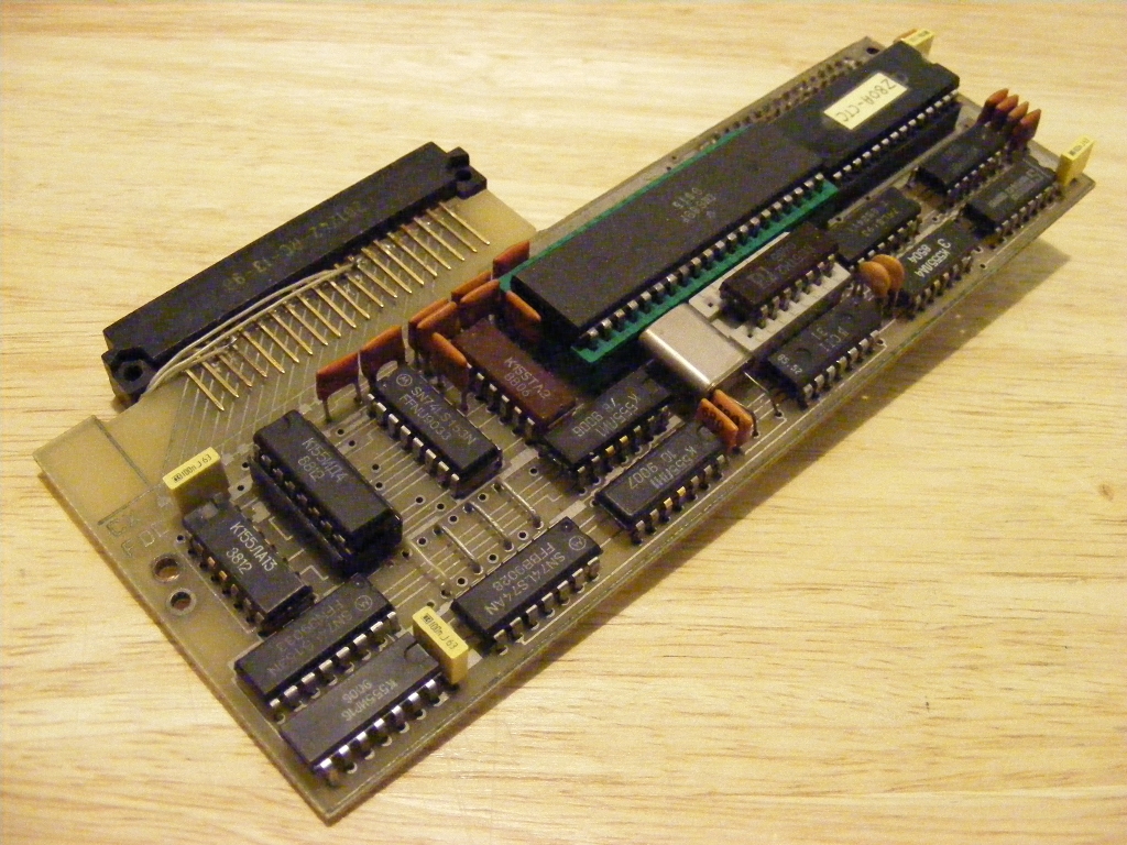
This is the initial version of the interface I built in the '90s. Its only drawback is that the signal mapping at the data connector to the drive is totally messed up. In order to use it with 5.25" or 3.5" drives I simply rewired all signals to the data connector and then I made a nonstandard cable for drives 0, 2 and 3.
Schematics - v.0
NOTE:
The original version of the floppy disk interface uses separate signals for SELECT, MOTOR ON (HEAD LOAD) and READY to 4 disk drives. The signal mapping to the pins of the floppy disk drive connector does not comply with the standards used by floppy drive manufacturers. As such, in the computers I built I had to remap the signals coming from the floppy interface to the pins of the floppy drive data connector (on the interface) in order to be able to use the drive. Then I made a modified data cable, having 3 connectors for 5 1/4" drives, on which some of the ground lines were separated from GND by extracting the pins in the connectors (on the cable) and then used to carry the now distinct signals for SELECT, MOTOR ON (HEAD LOAD) and READY to the drives.
Circuit board - v.0
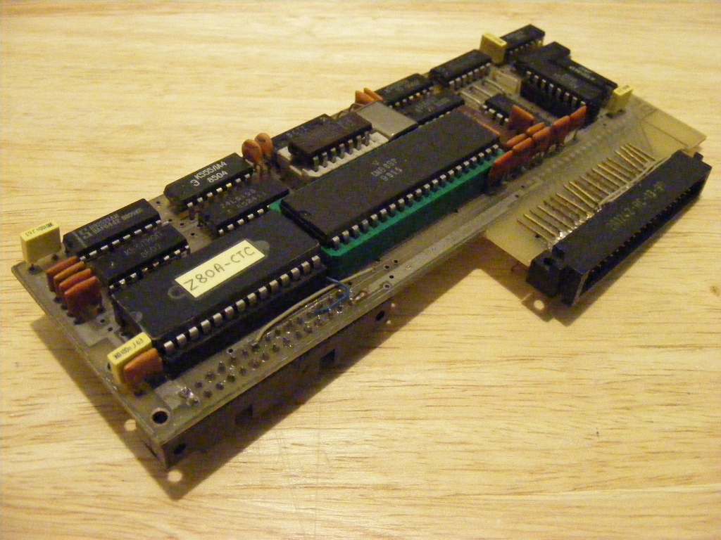
A few images of one of the 2 floppy interfaces built by me in the '90s:
On the top side, (component side) you can see 4 white wires connected to some of the pins of the floppy drive connector. All pins on this side of the connector should in theory be connected to GND, but these 4 pins have been hijacked form their original purpose and used for carrying the SELECT and MOTOR ON signals to 2 more drives aside from the first one, so this modified data cable could connect 3 distinct drives at the same time. The pins of the drive connectors on the cable were pulled out of the connector for these ground lines so that these extra signals would not be shorted to ground. The first connector on the cable had all 4 pins pulled out, the second connector had only 2 pins out and the last connector (the third) had no pin pulled out. Between the 3 conectors (that is in 2 intervals) the cable wires were cut, then each soldered to its neighboring wire which was going to the pin corresponding to the signal carried from the next drive connector.
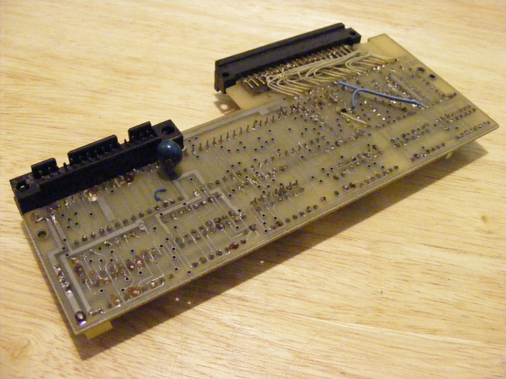
The 2 wires (a white one and a blue one) seen in the next image (also on the top side) at the connector for the mainboard, do not make up any modification, but I simply replaced some circuit board tracks which had come off the board.
In the next image, with the opposite side of the board, by the mainboard connector you can see a (blue) tantalum capacitor smoothing the power line to the interface, and beside it you can see the end of a blue wire coming out of a hole, which is the same blue wire mentioned above (on the other side) used for rebuilding a damaged circuit track. The other wire (white) can be seen coming out behind the connector, immediately right of the capacitor. Further to the right, you can see a white wire connecting two points about the middle of the board, I just used it to rebuild a circuit track previously cut by me for testing purposes (the track between U04/9 and U03/3, NRDY). Next to this wire there is also a piece of bifilar cable soldered between U04/12 (signal NRDY2 from the C: drive) and a pin of the connector to the floppy data cable. The bifilar cable is cut (as you can best see in the last image). I cut it when I started studying the boards in order to begin this project. At the missing end it had a simple switch. With it I was connecting and disconnecting the READY signal for the C: drive. I explain all this in order to make a point: the floppy interface working with the CoBra I built did not require basically any changes from the schematics in the original hardware manual. The original schematic is perfectly functional and needs no change, except for the mapping of signals to the floppy cable connector, which is completely nonstandard.
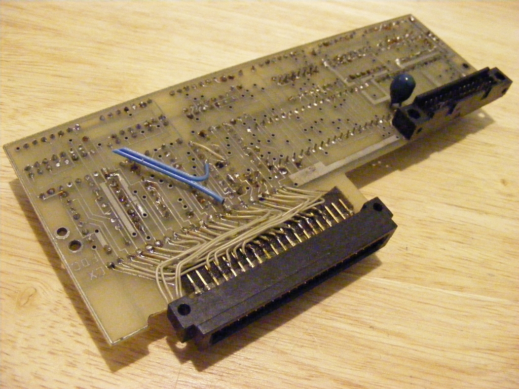
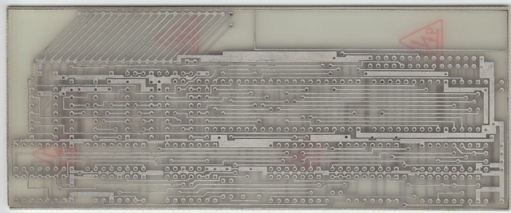
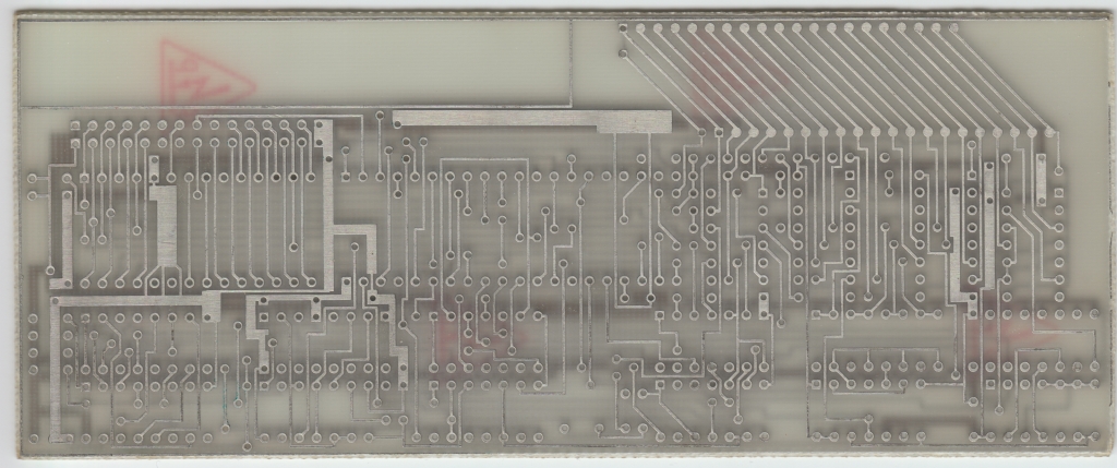
What you see below is a floppy interface board (unused) for CoBra, which until not long ago (that is about 2010) I believed was true, functional, well designed. I bought it (that is, spending some money on it, of course!) after I built the two CoBra computers I have (around 1992-1994), thinking that maybe someday I will assemble another interface. I never got to doing that - fortunately. Why "fortunately"? Because when I started the "CoBra Back to Life" project (in 2009), in order to make it easier to manually draw the board layout in PCB, I used as background the scanned image of this "original" unused floppy board (for the mainboard I used the B/W images from Roelof Koning, but Roelof did not have any images for the floppy interface). And when I finished drawing it using this board as a template I was surprised to see that it actually has a lot of mistakes and before anything VCC and GND are shorted to one another !!! So if I had made the fatal mistake of soldering parts on this mainboard, I would have been grieving afterwards. I don't see any explanation for this "phenomenon" board, other than the ill-intentioned people who manufactured it slipped fatal errors on it on purpose. Even Vasile Prodan is suspicious about their intentions, so this is very likely the truth.
Top side (components):
Bottom side (solder):
Comparing this side to the previous images (of the assembled functional interface) a difference can be noticed on the left end (in the image below there is a short wide track, vertical, which shorts VCC to GND).