- CCC with a value of 560 pF (pag.1 - Memory access prioritizer and command logic),
- C49 with a value of 330 pF (pag.3 - Configurator and selector circuit, the 80K RAM modification)
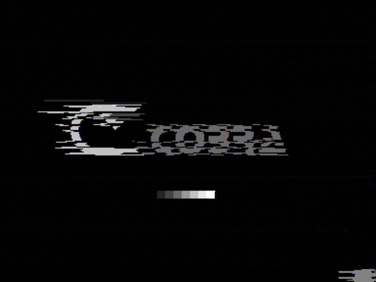
The absence of this capacitor was causing the kind of behaviours (in Basic and Devil) shown in the snapshots below:
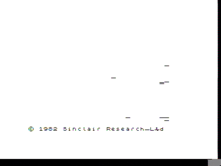
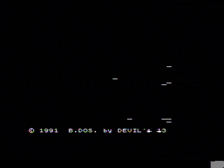
- A capacitor not prescribed by the schematics but whose necessity was experimentally determined, with a value of 150 pF, connected directly to pins 4 of dynamic memories (banks #0, #2 and #3) in order to add a delay to RAS (and as a side effect to CAS too) for the system memory. (pag.8 - "Dynamic memory circuit - pag.1/2"). Basically a capacitor to adjust the timing for RAS and/or CAS to memory in order to correctly access the dynamic memory (system memory). This capacitor was required when using MMN4164-3 chips for the system memory (manufactured at Microelectronica). I don't know for sure what is their access time, but the catalogue says it's between 200 and 300 ns. Afterwards I also did tests using TMS4164-20 DRAM memories for the system memory. Well, with these I did not have to use any kind of delay capacitors on RAS or CAS to the system memory. Hence I concluded that 200 ns access time memories are the ideal DRAM memories for CoBra. I will open a little bracket here in order to show the screenshot below, depicting what will be shown on the screen when access to the system memory is not properly tuned and loading Basic, Devil, Opus or anything like that is attempted using the "B" key from the startup configuration:
- A 150 pF capacitor (also not prescribed by the schematics), connected to 3 of U36 (pag.3 - "Configurator and selector circuit"). This was required to delay the RFSH signal so that the falling edge of BNRFSH from the CPU would get to the clock input U36/3 (negated through U53/2) AFTER bit 7 of register R in the CPU became available and stable on the BA7 address line. To explain in more detail, I will quote what the CoBra hardware manual says: at power up, in the startup configuration, register R in the CPU has bit 7 set to 1. Then, when a key is pressed indicating the operating system chosen next, this bit is reset to 0 and appears on address line BA7 of the address bus during the first refresh cycle after the instruction who reset it. The moment is marked by the activation (transition to "0") of the RFSH signal generated by the CPU. This falling edge of BNRFSH is negated by U53/2 and transformed in rising edge for the clock input of flip-flop U36 (7474 uses rising clock edges). So the falling edge of BNRFSH should load flip-flop U36/5+6 with the data bit supplied on the address line BA7. The problem is that if we check the official documentation of Z80, we learn that (see the image below extracted from the manual, last half of the M1 cycle) the refresh addresses (BA0-BA7) are not guaranteed to be stable except during MREQ activation time. MREQ is activated half a CPU clock period after RFSH is activated, and RFSH is activated simultaneously with refresh addresses becoming available on the address bus.
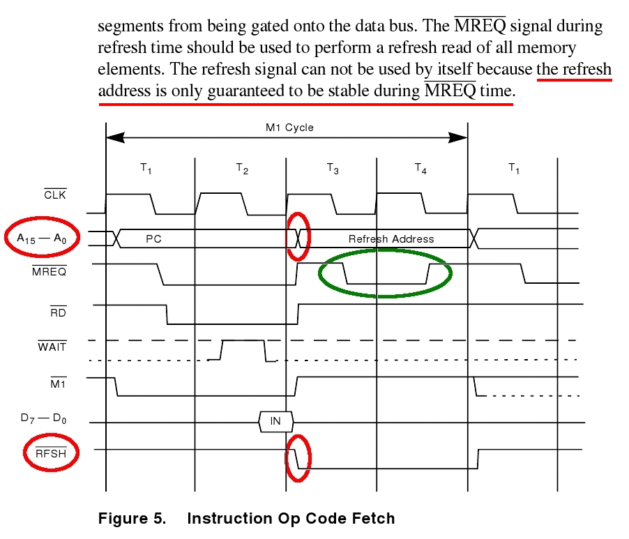
In other words, the falling edge of RFSH occurs too early to sample the refresh address on the address bus because this address is only guaranteed to be stable half a CPU clock period later. The truth is, the CoBra schematics have inverter U53 inserted on BNRFSH before U36, and BA7 is takedn directly to U36, so BNRFSH already has some delay from BA7, which in the case of both mainboards assembled by me back in the 90's was sufficient to ensure a correct operation. But now, when I built this prototype, for some reason this delay was not sufficient anymore, and my practical problem was that when pressing the "D" key in the startup configuration in order to load CP/M from disk, the border would only flash once briefly to blue, come back to black and then the computer would freeze, not reading any more keys and the disk drive would not spin the disk to read it. That because signal LO6, instead of staying at "1" for the CP/M configuration, would go to "0", which was visualized with the logical probe. Fortunately, on the forum I met YO3GHM who had the patience and kindness to analyze my problem and came up with the delivering solution, a delay capacitor on U36/3 (experientia docet...). As soon as I applied it, the mainboard started loading the disk operating system correctly. The interesting fact is that in DEVIL (BASIC using floppy disk for CoBra) disk operations would take place perfectly, commands CAT and LOAD had no problems. That's because LO6 had no problems switching to "0" (for the BASIC/DEVIL hardware configuration) but only had problems staying at "1" (for the CP/M hardware configuration).
;)
;)
;)